Introduction:
The TDA2009A Stereo Audio Amplifier Circuit is a widely used amplifier design for medium-power audio amplification. The TDA2009A is a dual audio power amplifier integrated circuit (IC), capable of delivering up to 12 watts per channel when connected to a suitable power supply and a 4Ω speaker load. This circuit is commonly implemented in home audio systems, portable audio equipment, and DIY audio amplifier projects.
This particular configuration is a stereo amplifier, meaning it can drive two separate audio channels (left and right), making it suitable for applications requiring stereo sound output. The IC is known for its high output power, thermal stability, low distortion, and easy-to-use design.
The TDA2009A Stereo Audio Amplifier Circuit is a versatile and cost-effective solution for audio amplification in medium-power applications. It is widely used in DIY audio projects, home audio systems, and portable speaker setups due to its compact design, thermal protection features, and ability to deliver clean, distortion-free stereo sound output. This circuit can amplify low-level audio signals and drive two speakers, making it ideal for applications requiring enhanced stereo sound performance. Additionally, its simplicity and efficiency make it a popular choice among hobbyists and audio enthusiasts alike, providing up to 12W per channel with minimal external components.
Components Required
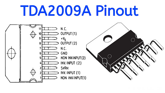
TDA2009 Pinout:
The TDA2009A is a dual power amplifier IC designed specifically for stereo audio amplification. Manufactured by STMicroelectronics, this IC is highly regarded for its compact design and ability to deliver high power output with minimal external components. It is commonly used in audio applications such as home audio systems, car stereos, and DIY audio amplifier projects due to its efficiency and reliability.
Key Features:
- Dual Channel Amplification: The TDA2009A can independently amplify two channels, making it ideal for stereo applications. Each channel can output up to 12W of power when driving a 4Ω speaker.
- High Output Power: It can deliver up to 18W per channel when used with a suitable power supply and load, depending on the system configuration.
- Low Distortion: The IC features low Total Harmonic Distortion (THD), ensuring high-quality sound reproduction even at higher power levels.
- Thermal and Short Circuit Protection: It has built-in protection mechanisms to prevent damage in case of overheating or short circuits, which enhances the reliability of the amplifier.
- Wide Operating Voltage Range: The IC operates in a voltage range of 8V to 24V, making it adaptable for different power supplies, from battery-operated devices to mains-powered systems.
Circuit Diagram:

Circuit Working:
The working of this stereo audio amplifier circuit can be explained in the following steps:
- Power Supply Section:
- The circuit operates on a +8V to +24V DC power supply, providing the necessary voltage for the TDA2009A IC to function.
- Capacitors C3 (22uF), C4 (0.1uF), and C5 (100uF) stabilize the power supply by filtering any noise or ripples in the input DC voltage. These capacitors ensure smooth power delivery to the IC for optimal performance.
- Input Stage:
- The audio inputs for the left and right channels are connected to pins 5 (Left Input) and 1 (Right Input) of the TDA2009A IC.
- Coupling capacitors C1 (2.2uF) and C2 (2.2uF) are used at the input stage to block any DC component that may be present in the input signal, allowing only the AC audio signal to pass through.
- These signals are then fed into the amplifier's input stage for processing.
- Amplification Stage:
- The TDA2009A amplifies the incoming low-level audio signals, using its internal circuitry to boost the signal power.
- The resistors R1 (1kΩ), R2 (18Ω), and R3 (1Ω) form part of the feedback network, which controls the gain and stability of the amplifier in the left channel. Similarly, R4, R5, and R6 perform the same role for the right channel.
- Capacitors C6 (220uF) and C9 (220uF) in each channel filter out noise from the feedback signal, ensuring that the output is clean and stable.
- Bypass capacitors C7 (0.1uF) and C10 (0.1uF) filter out high-frequency noise that may affect the amplifier's performance.
- Output Stage:
- The amplified audio signals are sent to the speakers via output coupling capacitors C8 (2200uF) and C11 (2200uF), which block any DC components from reaching the speakers.
- The left and right audio signals are directed to L SPK and R SPK respectively, where they are converted into sound.
- The large output capacitors ensure that the DC component does not damage the speakers and only the amplified AC signal reaches them.
- Thermal and Short Circuit Protection:
- The TDA2009A IC has built-in protections, including thermal shutdown and short-circuit protection, ensuring the amplifier does not get damaged under high-load or faulty conditions.
Applications:
- Home Audio Systems: Suitable for amplifying audio signals from various sources such as CD players, media players, or TV sets.
- Car Audio Systems: The IC’s compact size and high output make it ideal for use in automotive audio amplifiers.
- DIY Audio Projects: Popular among hobbyists due to its ease of use, minimal external components, and low cost.
Conclusion:
This stereo amplifier circuit using the TDA2009A is an efficient and reliable design for medium-power audio applications. Its ability to drive two channels of audio makes it ideal for stereo systems. With proper power supply, speaker, and input connections, this amplifier can provide clear and powerful sound output suitable for various audio applications.

